
TECHNOLOGY
Limitation of Si-based ICs
Silicon-based integrated circuits (ICs) have been the foundation of electronics for several decades, but they are reaching their physical limitations in terms of miniaturization and power efficiency. As the demand for smaller, more powerful devices continues to grow, silicon-based ICs can no longer keep up.
This means that further progress in the industry will require the development of new materials and technologies to make the next generation of electronic devices possible.
Two-dimensional materials
Two-dimensional (2D) materials are substances with a thickness of one to a few atoms. These materials are a promising solution to the physical limits of silicon-based ICs, including graphene (with an extremely high electron mobility (350’000 cm2/V/s at room temperature), hexagonal boron nitride (h-BN), MoS2 and other ultra-thin substances. Such 2D materials are used in many applications, including electronics, photovoltaics, filtration and DNA translocation, single photon emitters and other quantum devices. The 2D semiconductors have unique properties (highly conductive, flexible and transparent) that make them attractive for use in next-generation electronic devices, which could enable new designs and functionalities that aren’t possible with silicon.

However, 2D electronic devices require an encapsulation material to serve as a protective layer, shielding them from environmental damage and potential harm caused by other materials. h-BN, a highly effective encapsulation material, offers unparalleled protection to 2D electronic devices. In addition, this layer also serves as an insulator, further enhancing the performance and stability of the devices.

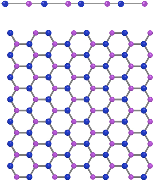
Hexagonal boron nitride
Hexagonal boron nitride, commonly referred to as h-BN (also called as white-graphene), is a remarkably versatile 2D material composed of boron and nitrogen atoms. With exceptional electrical insulating capabilities, excellent thermal conductivity, extraordinary chemical stability, good mechanical properties, and exceptional optical properties, h-BN is an ideal material for use as an encapsulation material in 2D electronic devices. Its unique properties offer unmatched protection against environmental damage and harmful materials, making it a perfect choice for both electronic and chemical shielding.
The unique properties of h-BN including:
- Excellent electrically insulating
- large band gap: 6.0 eV
- high dielectric strength (> 10 kV/mm)
- low dielectric loss
- low dielectric constant (~ 4)
- High thermal conductivity
- in-plane thermal conductivity as high as ~ 550 W/m K at room temperature
- 20x better than SiO2
- low coefficient of thermal expansion (< 2.3 x10⁻⁶/°C)
- thermal shock resistant
- Extraordinary chemical stability
- inert – oxidation resistant up to 850ºC in air, 2000ºC in inert atmospheres (steel processing and ceramic manufacturing)
- resistant to corrosion by most molten metals (coating applicaitons)
- non-toxic (use in cosmetics)
- dopant source
- Good mechanical properties
- low density (2.2 g/cm3), can be used in aerospace applications
- low coefficient of friction (excellent lubricity)
- low hardness
- Exceptional optical properties
- high refractive index (1.65)
- high transparency in the visible spectrum (applications in sensors and displays)
Absence of high-quality h-BN at wafer scale
Despite the scalability of 2D semiconductors, the absence of high-quality h-BN at wafer scale on the market poses a significant challenge for the mass production of 2D electronic devices. Although research labs can produce high-quality h-BN in small scales (micro-meter range), commercial-scale production has proven to be a bottleneck due to the lack of scalable manufacturing processes. That’s where SwissBN comes in: to overcome this hurdle and enable the large-scale production of high-quality h-BN. By providing a reliable source of high-quality h-BN, SwissBN could unlock the full potential of 2D electronic devices.